Reading Circuit Schematics is one of the most important skills every electronics student, engineer, and hobbyist should master. Every electronic device—from a simple LED circuit to a modern smartphone—is designed using schematic diagrams that follow international standards.
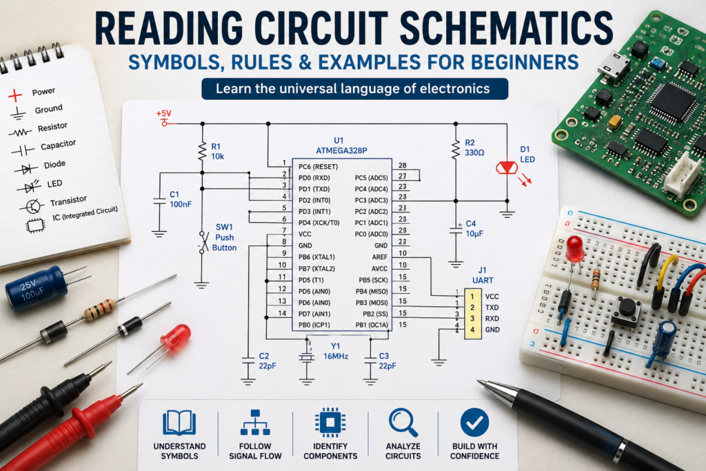
Table of Contents
Introduction
A circuit schematic is a standardised map of a circuit, showing every component and connection using agreed symbols. Being able to read schematics is non-negotiable — every project, datasheet, and repair manual uses them. The good news: there are only about 30 symbols you need for 95% of all electronics work.
Before starting this lesson you should know:
After reading this guide you’ll be able to:
✔ Read standard schematic symbols
✔ Understand wire connections
✔ Identify ICs and transistor symbols
✔ Follow signal flow
✔ Avoid common beginner mistakes
✔ Read simple electronic schematics confidently
Part 1: The Ground Rules for Schematics
- A schematic is not a picture of a physical circuit — it’s a logical map.
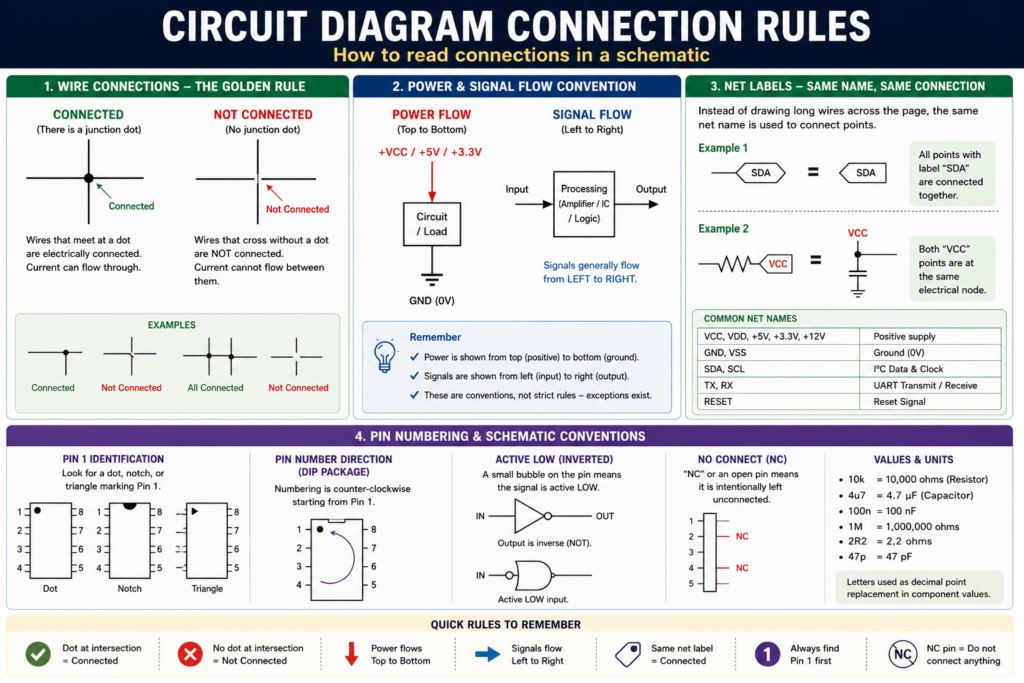
- Lines represent wires. A junction dot (•) where lines cross means they’re connected. Lines crossing without a dot are NOT connected.
- Power flows from top to bottom by convention (VCC/5V at top, GND at bottom).
- Signals generally flow left to right (input on left, output on right).
- Every wire with the same label anywhere on the schematic is connected, even if not drawn as a physical line.
- Component values and labels are written next to each component.
⚠ Common Mistake
Many beginners think crossing wires automatically connect.
Remember:
Crossing without a junction dot = NOT connected.
Crossing with a junction dot = Connected.
Part 2: Essential Schematic Symbols
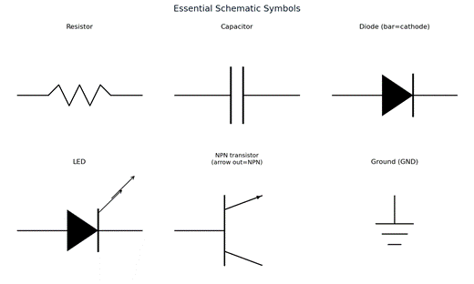
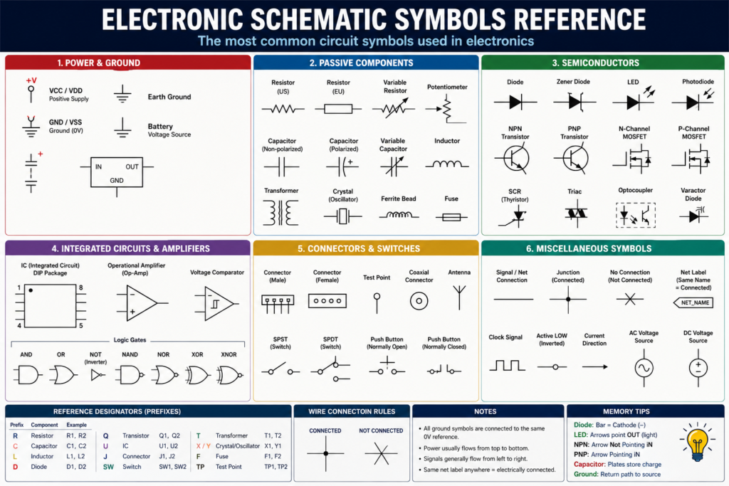
Figure 1 — Core schematic symbols you’ll see in nearly every diagram.
Power and Ground Symbols
| Symbol Name | What it means | Common labels |
| VCC / VDD | Positive power supply voltage | VCC, VDD, +5V, +3.3V, +12V |
| GND / VSS | Ground (0V reference) | GND, VSS, ⏚ (earth symbol) |
| Battery | Voltage source with cells | BAT, B1 |
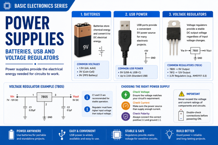
| Voltage regulator | Stabilised power output | Shown as component or labelled |
Passive Component Symbols
| Component | Symbol appearance | Label format |
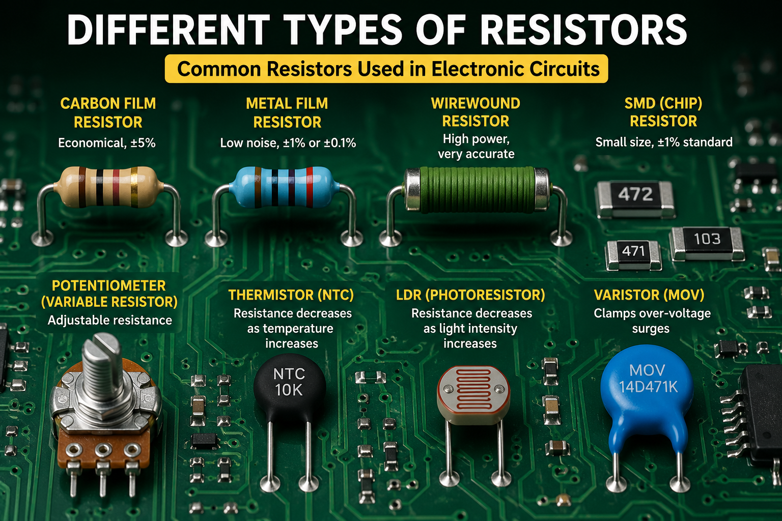
| Resistor | Rectangle (European) or zigzag (US) | R1 = 220Ω or R1 = 4.7kΩ |
| Capacitor (non-polarised) | Two parallel lines | C1 = 100nF |
| Capacitor (polarised) | One curved plate (negative) | C2 = 100µF 25V, + marked |
| Inductor | Loops or bumps on a line | L1 = 10µH |
| Transformer | Two coupled inductors | T1, ratio shown |
| Crystal | Rectangle with lines | X1 = 16MHz |
Semiconductor Symbols
| Component | Symbol key features | How to identify orientation |
| Diode | Triangle pointing in current direction, bar at cathode | Bar = cathode = − |
| Zener diode | Same as diode but bar has bent ends | Same as diode |
| LED | Diode with two arrows pointing away (light emission) | Arrows = light output |
| NPN transistor | Arrow on emitter points OUT (away from base line) | E arrow out = NPN |
| PNP transistor | Arrow on emitter points IN (toward base line) | E arrow in = PNP |
| N-ch MOSFET | Gate separate from channel, arrow points in | For enhancement mode |
| P-ch MOSFET | Same but arrow points out | Bubble on gate sometimes |
Logic and IC Symbols
| Symbol | Meaning |
| Rectangle with VCC/GND/pins | Integrated circuit (IC) — pins numbered from pin 1 (dot or notch) |
| Op-amp triangle | Operational amplifier — + and − inputs on left, output on right |
| Logic gate shapes | AND, OR, NOT, NAND, NOR, XOR — each has specific curved shape |
| Multiplexer | Trapezoid shape with multiple inputs, one output |
| Clock signal | Square wave → into a pin means clock input |
| Bubble (circle) on pin | Active LOW — signal is inverted/active when LOW |
Part 3: Reading a Real Schematic — Step by Step
Step 1: Identify Power and Ground
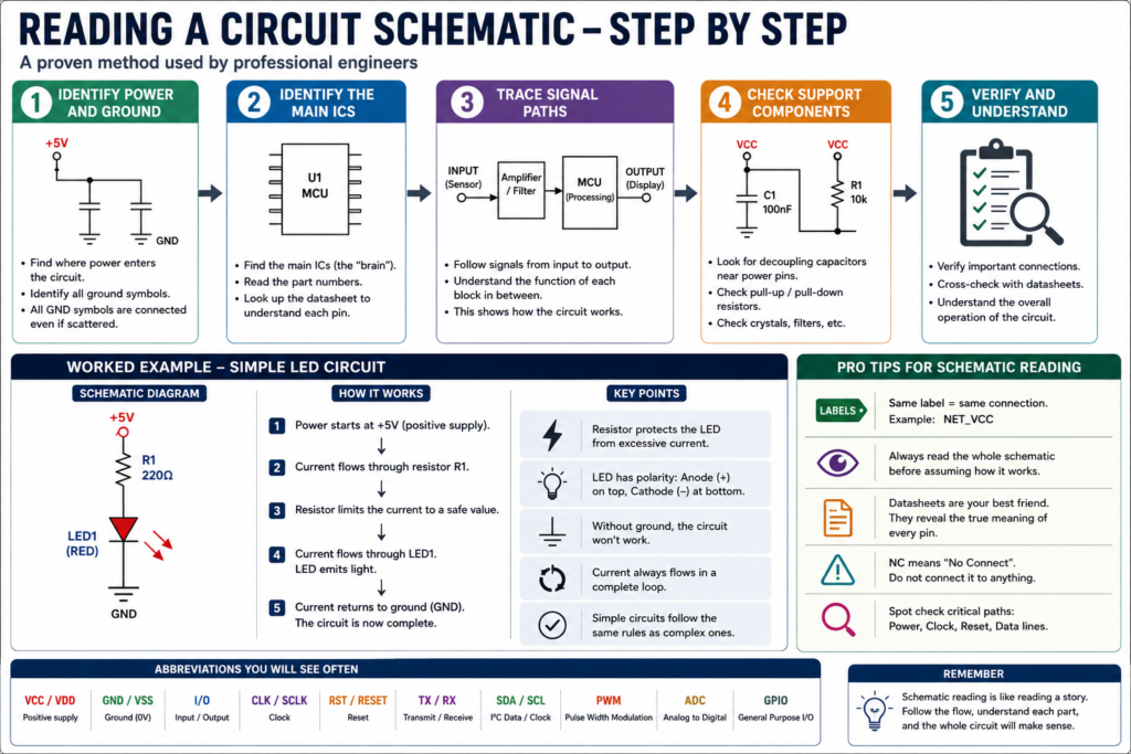
Find where power enters the circuit (VCC, battery, USB). Find all ground symbols — remember all GND symbols are connected even if scattered around the schematic.
Step 2: Identify the Main ICs
Find the main integrated circuits — the ‘brain’ of the circuit. Read their part numbers and look up the datasheet to understand what each pin does.
Step 3: Trace Signal Paths
Follow wires from input to output — from a sensor or input pin through amplifiers, filters, and digital circuits to the output (display, actuator, or transmission). Each block has a purpose.
Step 4: Check Support Components
Look for support components around each IC: decoupling capacitors near power pins, pull-up/pull-down resistors on I2C lines, crystal oscillator for clock, etc.
Part 4: Common Schematic Conventions and Tricks
- Net names: instead of drawing wires across a large schematic, label wires with the same name — UART_TX on two separate parts of the schematic means they’re connected.
- Power flags: in KiCad and other EDA tools, power pins need a ‘PWR_FLAG’ to tell the ERC that a net is intentionally connected to power.
- Pin 1 identification: ICs have a dot, notch, or triangle marking pin 1. Count counterclockwise from pin 1 for DIP packages.
- Values: always written next to the component — ’10k’ means 10,000Ω, ‘4u7’ means 4.7µF (the letter replaces the decimal point in European notation).
- NC: ‘No Connect’ — this pin is intentionally not connected. Don’t assume it’s ground.
✅ QUICK RECAP
Schematics use standardised symbols — not pictures of real components.
Junctions (dots) where lines cross = connected. No dot = wires cross but don’t connect.
Power flows top to bottom. Signals flow left to right (by convention).
Same label anywhere on a schematic = electrically connected.
Bar on diode = cathode. Arrow out of transistor = NPN. Bubble on pin = active LOW.
Read in order: power → main ICs → signal path → support components.
NC = No Connect. Don’t assume unconnected pins are GND.
Frequently Asked Questions
Q: Why do wires that cross on a schematic sometimes not connect?
A: Schematics are 2D logical maps, so wires often have to cross visually even when they belong to entirely separate nets. The presence (or absence) of a junction dot at the crossing point is the only thing that tells you whether they’re actually joined.
Q: How do I know which pin is pin 1 on an IC symbol?
A: Look for a small dot, notch, or index mark at one corner of the rectangle representing the chip. From there, pin numbers typically go counterclockwise around a DIP package, matching the physical notch on the real chip.
Q: What does it mean if a pin has a bubble drawn on it?
A: A bubble (small circle) on a pin indicates that signal is ‘active low’ — meaning the function it represents triggers when the pin is pulled LOW rather than HIGH. It’s common on reset and chip-select lines.
Q: Why are net names used instead of drawing every wire?
A: On complex schematics, physically drawing a wire from one side of the page to the other would create a tangled mess. Giving two or more pins the same net name achieves the same electrical connection while keeping the diagram readable.
Q: Is a schematic the same as a PCB layout?
A: No. A schematic shows the logical connections between components, without regard to their physical position. A PCB layout (covered in Post 13) shows where components actually sit on the board and how copper traces physically route between them.
Q: What should I do if I see an unlabelled ‘NC’ pin?
A: Leave it disconnected. ‘NC’ means the manufacturer has intentionally left that pin unconnected internally or wants it left floating — connecting it to ground or power without checking the datasheet first can cause unexpected behaviour or damage.
🚀 NEXT UP
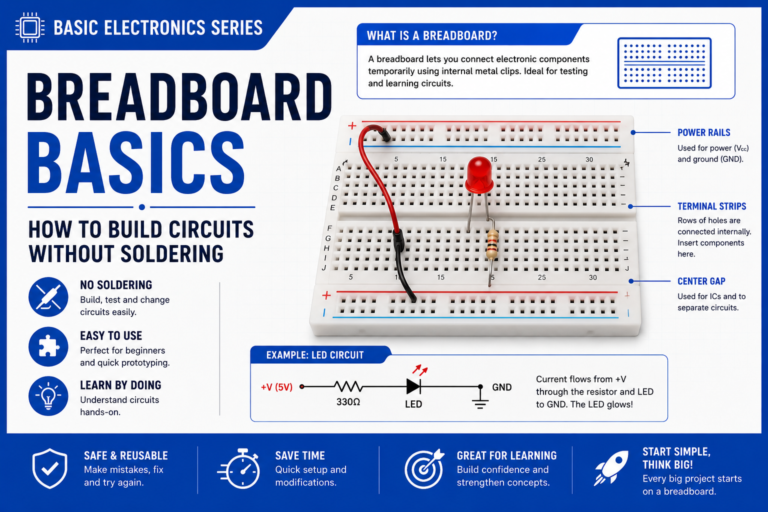
Post 11: Breadboard Basics — How to Build Circuits Without Soldering
Now that you can read a schematic, we translate it onto a breadboard — layout, common mistakes, and best practices.