POST 13 ● SERIES 1: ELECTRONICS BASICS ● 11 min read
How real electronics products are built — and how you can make your own PCB
Table of Contents
Introduction
Every electronic product you own — your phone, your Arduino, your laptop — is built on a PCB (Printed Circuit Board). A PCB replaces the mess of breadboard wires with permanent copper traces etched onto an insulating substrate: reliable, compact, manufacturable, and professional. This post explains what a PCB is, its types, how to read one like an engineer, and the path from breadboard prototype to manufactured PCB — cheaper and easier than ever for hobbyists.
Part 1: What is a PCB and Why Is It Important?
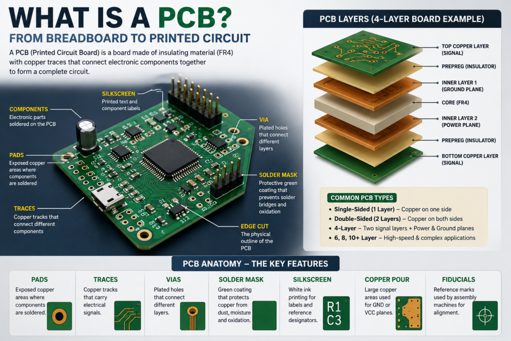
A PCB is a laminated sandwich of insulating material (usually fibreglass epoxy, called FR4) and thin copper layers. The copper is etched to form traces connecting component pads, just like wires in a breadboard, but permanent and in a fixed layout.
| Material | Properties | Used for |
| FR4 (fibreglass epoxy) | Standard PCB material, rigid, good insulation, flame-retardant | Most PCBs from consumer to industrial |
| FR2 (phenolic paper) | Cheaper, brown colour, not as strong | Very cheap consumer products |
| Aluminium core | Excellent heat dissipation, rigid | LED lighting, power electronics |
| Flexible (polyimide) | Bendable, thin | Wearables, internal cables, ribbon cables |
| Rogers PTFE | Very low dielectric loss at RF | Microwave, RF, antenna boards |

Figure 1 — Cross-section of a 4-layer PCB stack-up.
- Single-sided (1 layer): copper only on one side. Cheapest — very simple products.
- Double-sided (2 layers): copper on both sides connected through ‘vias’ (plated holes). Standard for hobby and most commercial boards.
- 4-layer: two outer layers + two inner layers with power planes for clean power distribution. Standard for MCU boards.
- 6, 8, 10+ layer: complex ICs, high-speed digital, phones, CPUs.
Part 2: PCB Anatomy — Reading a Board
| PCB Feature | What it is | Colour/Appearance |
| Pads | Exposed copper where components are soldered | Shiny silver/gold, no solder mask |
| Traces | Copper tracks connecting components | Hidden under green solder mask, visible as lines |
| Vias | Plated holes connecting different layers | Small circles, usually not component holes |
| Solder mask | Green (usually) coating protecting copper | The green colour of most PCBs |
| Silkscreen | White ink layer with component labels, ref designators | White text: R1, C3, U1, J2 |
| Copper pour | Large filled copper area, usually GND or VCC plane | Filled area visible as different shade |
| Edge cuts | The physical outline of the board | The edges of the PCB |
| Fiducials | Reference marks for assembly machines | Small circles often in corners |
Component Packages
Figure 2 — Through-hole vs surface-mount packages.
Through-hole (TH) component leads go through holes in the PCB and are soldered on the back — older, easier to hand-solder, physically robust (Arduino headers, DIP ICs, larger capacitors). Surface Mount (SMD/SMT) components sit on pads on the surface with no holes — smaller, faster to manufacture, lower cost in production (most modern ICs, resistors, capacitors).
| Package | Full name | Size | Where you see it |
| DIP-8, DIP-14, DIP-16 | Dual In-line Package | Large, through-hole | Classic ICs: 555, LM741, ATmega28 |
| SOP, SOIC | Small Outline IC | Medium SMD | Modern ICs on development boards |
| QFP, TQFP | Quad Flat Package | Medium SMD, fine pitch | STM32, AVR in production |
| QFN, LQFN | Quad Flat No-lead | Small SMD, no external leads | ESP32, nRF52 SoCs |
| BGA | Ball Grid Array | Very fine, balls underneath chip | Processors, RAM, FPGAs |
| 0402, 0603, 0805 | SMD resistors/capacitors | 0.4×0.2mm to 0.8×0.5mm | On almost every modern PCB |
Part 3: The PCB Manufacturing Process
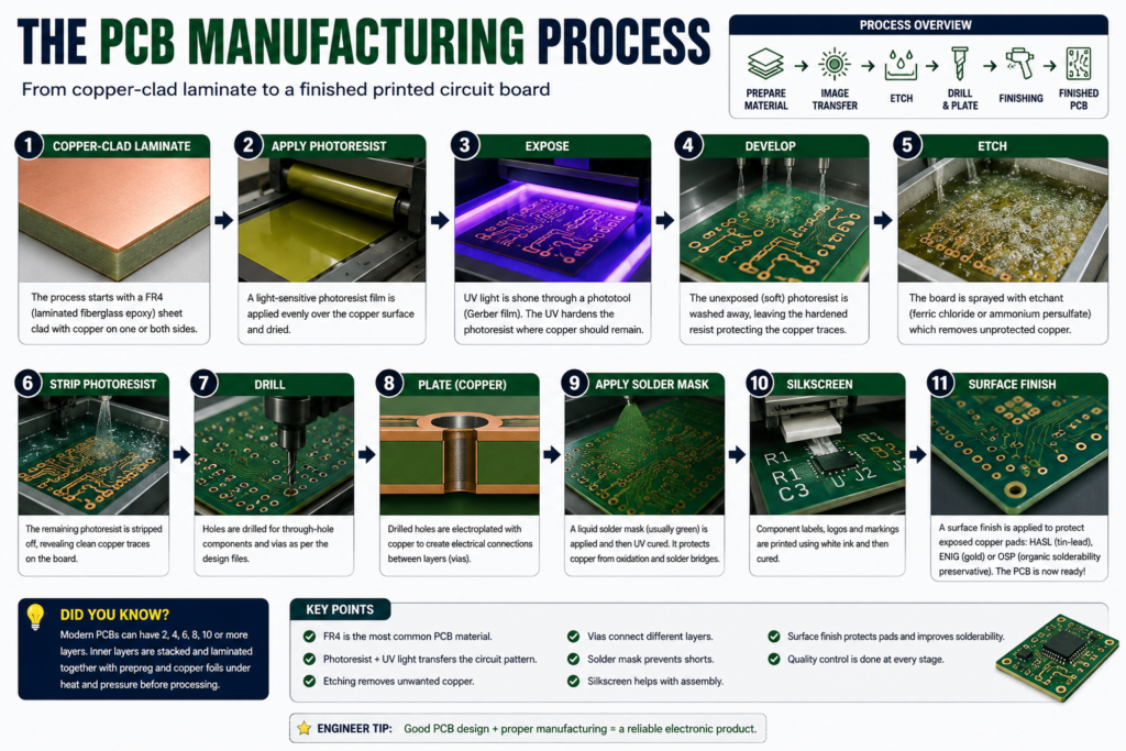
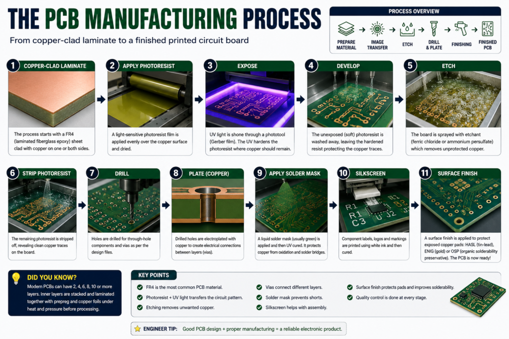
Figure 3 — The PCB manufacturing process flow.
1. Copper-clad laminate: start with FR4 sheet with copper on both sides.
2. Apply photoresist: coat copper with UV-sensitive film.
3. Expose: shine UV through a Gerber film negative — UV hardens photoresist where copper should stay.
4. Develop: wash away unexposed photoresist.
5. Etch: spray with ferric chloride or ammonium persulfate — dissolves exposed copper, leaving only the traces.
6. Strip photoresist: remove remaining film.
7. Drill: drill holes for vias and through-hole components.
8. Plate: copper-plate the drill holes to make electrical connections (vias).
9. Apply solder mask: coat with liquid solder mask (usually green), expose to UV.
10. Silkscreen: print component labels using white ink.
11. Surface finish: HASL (hot air solder levelling), ENIG (gold), or OSP to protect exposed pads.
Part 4: Designing and Ordering Your Own PCB
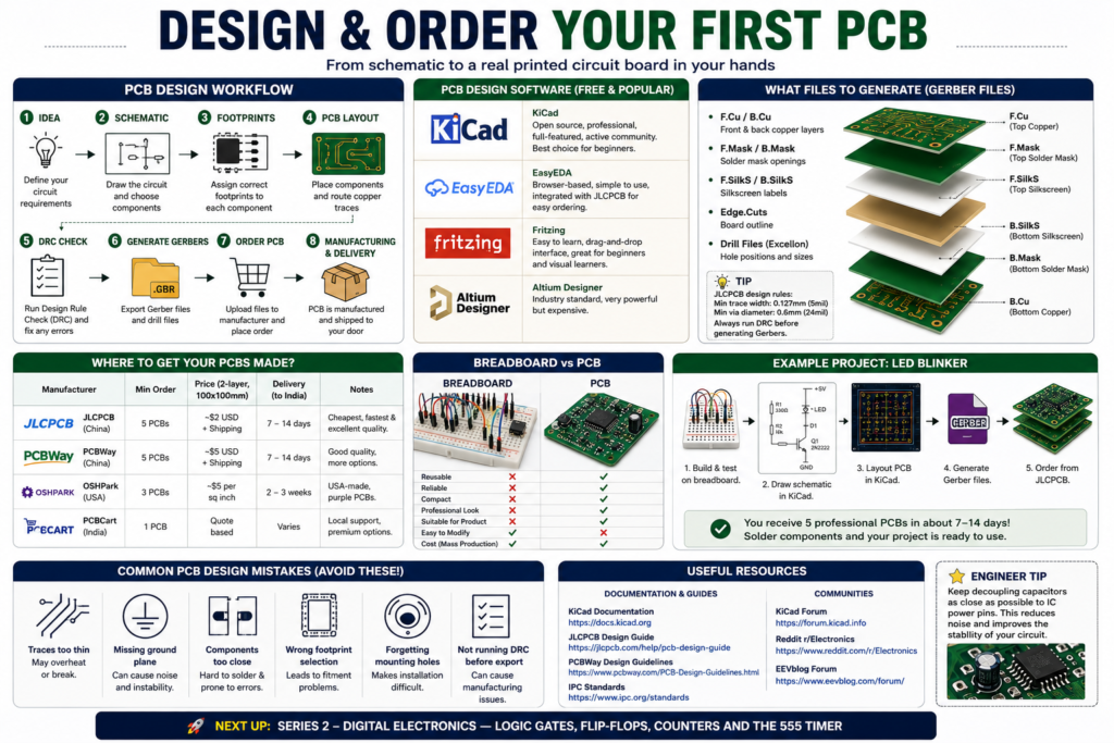
Free PCB Design Software
- KiCad: open source, professional, active community — best choice.
- EasyEDA: browser-based, simple, integrates with JLCPCB directly.
- Fritzing: visual, beginner-friendly, but limited.
- Altium Designer: industry standard but expensive.
Getting PCBs Manufactured
| Manufacturer | Min order | Price (2-layer, 100×100mm) | Delivery (to India) | Notes |
| JLCPCB (China) | 5 PCBs | ~$2 USD + shipping | 7-14 days | Fastest, cheapest, excellent quality |
| PCBWay (China) | 5 PCBs | ~$5 USD + shipping | 7-14 days | Good quality, more options |
| OSHPark (USA) | 3 PCBs | ~$5 per sq inch | 2-3 weeks | Purple boards, USA-made |
| PCBCart | 1 PCB | Quote based | Varies | More expensive, premium options |
What Files to Generate (Gerber Files)
To order a PCB, generate Gerber files from your design software describing each layer:
- F.Cu / B.Cu: front and back copper layers
- F.Mask / B.Mask: solder mask openings
- F.SilkS / B.SilkS: silkscreen labels
- Edge.Cuts: board outline
- Drill files (Excellon format): hole positions and sizes
💡 TIP
JLCPCB’s design rules: minimum trace width 0.127mm (5mil), minimum via diameter 0.6mm.
These are the constraints your PCB design must meet.
KiCad has a JLCPCB-specific design rules file you can download and import.
Always run the DRC (Design Rules Check) before generating Gerbers.
✅ QUICK RECAP
A PCB is a laminated sandwich of FR4 and copper layers, etched into permanent traces.
1, 2, 4, or more layers depending on circuit complexity.
Through-hole (TH): robust, hand-solderable. SMD: smaller, cheaper in production.
Manufacturing: photoresist → expose → etch → drill → plate → solder mask → silkscreen.
KiCad is the best free, open-source PCB design tool to start with.
JLCPCB/PCBWay make small-batch PCBs cheap and fast for hobbyists.
Always run DRC before generating Gerbers for manufacturing.
Frequently Asked Questions
Q: Do I need to know how to design a PCB before I can order one?
A: You do need a design file (Gerbers) generated from PCB design software like KiCad or EasyEDA. There’s a learning curve, but free tutorials and the active KiCad community make it approachable even for a first project.
Q: Why are PCBs green if the underlying copper is a different colour?
A: The green is the solder mask, a protective coating applied over the exposed copper traces to prevent unwanted solder bridges and oxidation. Solder mask is also available in other colours (red, blue, black, purple) — the colour is purely cosmetic and doesn’t affect function.
Q: What’s the real difference between through-hole and SMD components for a beginner?
A: Through-hole parts are much easier to hand-solder and more forgiving of mistakes, making them ideal while learning. SMD parts are smaller and often the only form available for modern ICs, but require finer soldering skill or hot-air/reflow techniques.
Q: How long does it actually take to get a PCB manufactured and delivered?
A: For a straightforward 2-layer board from a service like JLCPCB, the board itself can be fabricated in as little as 1-2 days; total delivery time to India is typically 7-14 days once international shipping is included.
Q: What is a via and why does a PCB need them?
A: A via is a small plated hole that electrically connects copper traces on different layers of the board. Multi-layer PCBs need vias so that a signal or power connection can move from, say, the top layer to an inner ground plane or the bottom layer.
Q: Can I go straight from a breadboard prototype to a PCB, or do I need an intermediate step?
A: You can go straight to a PCB once you’re confident the design works, but many people use stripboard or perfboard as an intermediate, low-risk step to validate a soldered version before committing to a fixed PCB layout that’s expensive to change.
🚀 NEXT UP
Series 2: Digital Electronics — Logic Gates, Flip-Flops, Counters and the 555 Timer
With the analog and passive component foundations in place, Series 2 takes you into the digital world: binary logic, gates, and the building blocks of computers.